Microsoft-Backed Startup Lace Raises $40M for Helium Atom Beam Lithography: What It Means for AI Content & Chip Design
Microsoft-Backed Startup Lace Raises $40M for Helium Atom Beam Lithography: What It Means for AI Content & Chip Design
Source: ETTelecom (March 24, 2026)
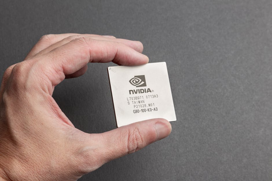
Lace, a Norway-based semiconductor manufacturing startup backed by Microsoft, has secured $40 million in Series B funding to commercialize its groundbreaking helium atom beam lithography technology. This investment, led by Nordic Alpha Partners and supported by Microsoft’s Climate Innovation Fund, signals a major push to overcome the physical and economic limits of current extreme ultraviolet (EUV) lithography, which is essential for manufacturing the advanced processors that power modern AI models and content creation tools. The development promises a future where more powerful, efficient, and specialized AI chips become cheaper and more accessible, directly impacting the capabilities and cost of AI-powered content automation platforms like EasyAuthor.ai.
Breaking the 2nm Barrier: How Helium Atom Beam Lithography Works

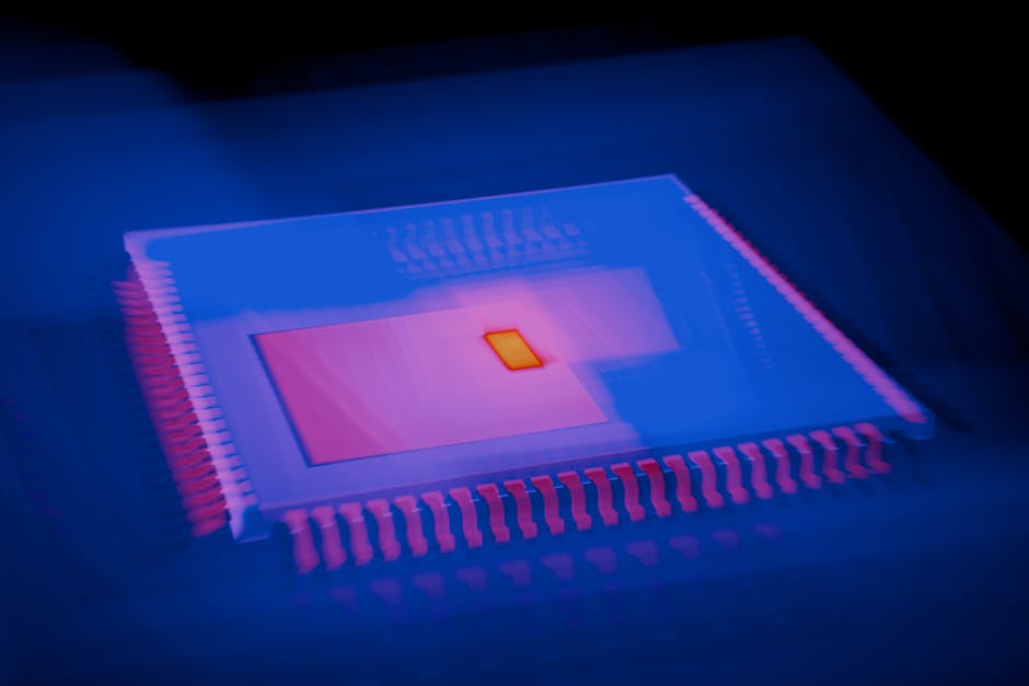
Current semiconductor manufacturing relies on photolithography, where light is used to etch circuit patterns onto silicon wafers. The most advanced technique, EUV lithography, uses 13.5-nanometer wavelength light. Pushing beyond the 2nm node with EUV is becoming exponentially more difficult and costly due to physics limitations like light diffraction and the need for complex multi-patterning.
Lace’s technology represents a paradigm shift. Instead of light, it uses a beam of neutral helium atoms. The core advantages are foundational:
- Atomic-Scale Precision: Helium atoms have a de Broglie wavelength thousands of times smaller than EUV light, enabling theoretically sub-atomic patterning resolution. This allows for the creation of chip features below 1nm.
- Zero Charging Damage: Unlike electron beams, neutral helium atoms do not electrically charge the photoresist or the wafer. This eliminates a major source of defects and simplifies the manufacturing process.
- Direct-Write Simplicity: The technology functions as a direct-write system, potentially reducing the number of process steps compared to complex EUV multi-patterning. This could drastically shorten chip design-to-production cycles.
- Material Versatility: The beam can pattern on a wider range of materials beyond traditional silicon, opening doors to novel chip architectures using 2D materials like graphene.
The $40 million investment will be used to scale the technology from lab prototypes to pre-production tools for chipmakers. While not replacing EUV fabs overnight, Lace aims to integrate its tools into existing production lines for specific, high-value layers where its atomic precision offers a decisive advantage.
The Direct Impact on AI Content Creation and Automation

For AI content creators, strategists, and bloggers, the silicon that runs AI models is the invisible engine of their work. Advances in chip manufacturing directly translate to more powerful, efficient, and affordable AI tools. Here’s how Lace’s breakthrough could reshape the landscape:
- More Powerful Local AI Models: Next-generation chips built with atom-scale precision will pack more transistors and specialized AI cores (NPUs, TPUs) into the same space. This enables more sophisticated large language models (LLMs) and diffusion models to run locally on devices, reducing reliance on cloud APIs, lowering latency, and enhancing privacy for content creation workflows.
- Lower Cost of AI Inference: If helium beam lithography reduces manufacturing complexity and increases yield, the cost of producing advanced AI accelerators (like those from Nvidia, AMD, or custom ASICs) could fall. This would reduce the operational costs for AI service providers, potentially leading to lower subscription fees for platforms offering AI writing, image generation, and SEO automation.
- Specialized AI Chips for Content Tasks: Easier and cheaper fabrication of custom chip designs (ASICs) allows for hardware optimized for specific content tasks—e.g., a chip designed solely for ultra-fast natural language generation or real-time SEO analysis. This specialization could lead to a new generation of hyper-efficient content creation tools.
- Energy Efficiency for Sustainable Scaling: Microsoft’s Climate Innovation Fund involvement highlights the energy angle. More efficient transistors mean AI model training and inference consume less power. For content farms or agencies scaling AI output, this translates to a lower carbon footprint and reduced compute costs, making large-scale content automation more sustainable.
In essence, the leap from light-based to atom-based lithography is not just a manufacturing story; it’s an enabler for the next wave of AI applications that content professionals will use daily.
Strategic Actions for AI Content Creators and Businesses
While commercial helium beam lithography chips are likely 5-7 years away, forward-thinking content businesses and creators should start positioning themselves now. Here are practical, actionable steps:
1. Future-Proof Your Tech Stack
Evaluate your current AI content tools based on their architecture and scalability. Prioritize platforms that:
– Offer API access for easy integration with future, more powerful local AI models.
– Are built on modular, open standards (like OpenAI’s API compatibility) to avoid vendor lock-in.
– Demonstrate a clear roadmap for leveraging hardware acceleration. Ask providers like Jasper, Copy.ai, or your custom GPT solution about their plans for on-device AI and hardware optimization.
2. Invest in Hardware-Aware Content Workflows
The divide between cloud and local AI processing will widen. Design your content pipelines accordingly:
– Use cloud-based models (GPT-4, Claude 3) for heavy, creative lifting like long-form article ideation and drafting.
– Shift editing, optimization, and publishing tasks to faster, cheaper local models running on your own hardware. Tools like Ollama for local LLMs or Stable Diffusion for images are precursors to this trend.
– Plan for a hybrid model where sensitive or time-critical tasks are handled locally, while massive batch jobs use the cloud.
3. Monitor the Semiconductor Startup Ecosystem
Lace is not alone. Track other disruptive chip tech startups (e.g., in optical computing, neuromorphic chips, or 3D stacking) through tech news aggregators or newsletters like Semiconductor Engineering or The Information. Understanding these trends helps you anticipate leaps in AI capability that could give you a competitive edge in content quality or production speed.
4. Advocate for and Develop Specialized AI Models
The coming wave of specialized AI hardware will perform best with specialized software. If you have development resources:
– Start fine-tuning open-source LLMs (like Llama 3 or Mistral) on your proprietary content data and style guides.
– Explore quantizing these models to run efficiently on current and future hardware.
– The goal is to have a perfectly tuned, efficient model ready to deploy on next-gen chips the moment they become available, bypassing generic AI tools.
5. Budget for a Hardware Refresh Cycle
While immediate spending isn’t necessary, factor a significant hardware upgrade into your 3-5 year business plan. The computers and servers you buy in 2027-2028 will likely contain the first generation of chips influenced by these new manufacturing techniques, offering a tangible performance boost for AI-assisted work.
Conclusion: From Atoms to Articles
The $40 million bet on Lace’s helium atom beam technology is a clear signal that the semiconductor industry is aggressively seeking the next foundational technology to keep Moore’s Law alive. For professionals in the AI content creation space, this is not a distant, abstract development. It is the roadmap to the tools of tomorrow: faster, cheaper, more powerful, and more specialized AI that will run the content engines of the future.
The strategic takeaway is to build agile, hardware-aware content operations today. By understanding the silicon trajectory, you can make informed choices about your software, workflows, and investments, ensuring you are ready to harness the full potential of atomically precise computing to create superior content at scale. The future of content isn’t just written in code; it’s etched in silicon, one helium atom at a time.